Verification of Charge Transfer in Metal-Insulator-Oxide Semiconductor Diodes via Defect Engineering of Insulator

Proposed mechanisms for the different distributions of defects in the

On Practical Charge Injection at the Metal/Organic Semiconductor Interface

Role of defects on the transparent conducting properties of binary metal oxide thin film electrodes - ScienceDirect

Figure 3 from Charge Trapping Memory Characteristics of Amorphous-Indium–Gallium–Zinc Oxide Thin-Film Transistors With Defect-Engineered Alumina Dielectric

Electron-Transport Characteristics through Aluminum Oxide (100) and (012) in a Metal-Insulator-Metal Junction System: Density Functional Theory-Nonequilibrium Green Function Approach. - Abstract - Europe PMC
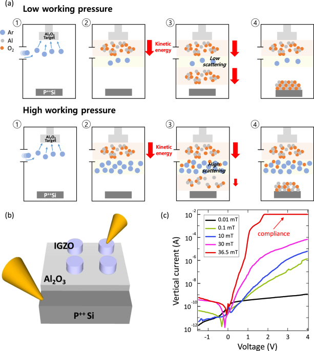
Current transport characteristics and schematic diagram of MIOS diodes

PDF) Verification of Charge Transfer in Metal-Insulator-Oxide Semiconductor Diodes via Defect Engineering of Insulator

Ion-gating analysis on conduction mechanisms in oxide semiconductors - ScienceDirect

a) XPS results for TiON film prepared via a single-step sputtering

Role of defects on the transparent conducting properties of binary metal oxide thin film electrodes - ScienceDirect

Role of defects on the transparent conducting properties of binary metal oxide thin film electrodes - ScienceDirect

Role of defects on the transparent conducting properties of binary metal oxide thin film electrodes - ScienceDirect