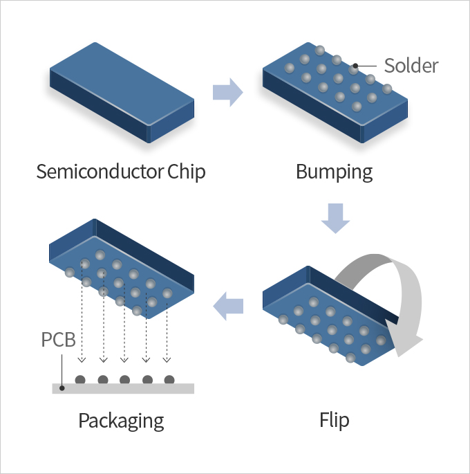
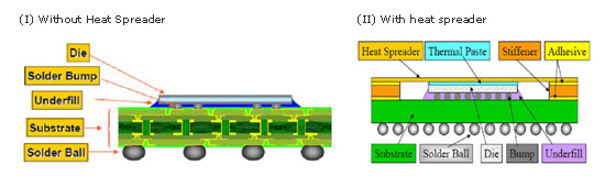
Schematic of the chip/bump build-up cross-section.

Materials, Free Full-Text

Figure 1 from A challenge of 45 nm extreme low-k chip using Cu

Polymers in Electronic Packaging: Build-Up Films for Flip Chip

Hybrid Bonding Process Flow - Advanced Packaging Part 5

Schematics of chip assembly by: (a) Au stud bump with conductive

High-performance, power-efficient three-dimensional system-in
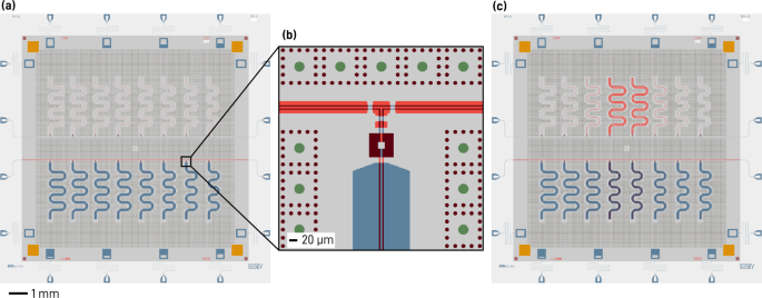
Improved parameter targeting in 3D-integrated superconducting
Levels and Steps of Integration. Introduction, by Suny Li
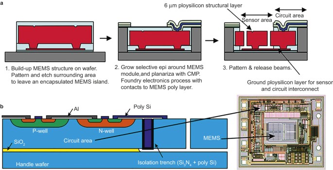
Integrating MEMS and ICs Microsystems & Nanoengineering

Multiple System and Heterogeneous Integration with TSV-Interposers

SEM image of a cross section of an unstressed 30 μm solder bump

15544557.ppt
Package Substrate, SAMSUNG ELECTRO-MECHANICS

Ball Grid Array (BGA) Packages and PCB Design Guidelines
Faraday Technology Corporation-Flip-Chip Package