MF181000 - SEMI MF1810 - Test Method for Counting Preferentially Etche

Defects on or in silicon wafers may adversely affect device performance and yield. Crystal defect analysis is a useful technique in troubleshooting device process problems. The type, location, and density of defects counted by this Test Method may be related to the crystal growth process, surface preparation, contamination, or thermal history of the wafer. This Test Method is suitable for acceptance testing when used with referenced standards. This Test Method describes the technique to count the density of surface defects in silicon wafers by microscopic analysis. Application of this Test Method is limited to specimens that have discrete, identifiable artifacts on the surface of the silicon sample. Typical samples have been preferentially etched according to SEMI MF1809 or epitaxially deposited, forming defects in a silicon layer structure. Wafer thickness and diameter for this Test Method is
Defects on or in silicon wafers may adversely affect device
performance and yield.
Crystal defect analysis is a useful technique in
troubleshooting device process problems. The type, location, and density of
defects counted by this Test Method may be related to the crystal growth
process, surface preparation, contamination, or thermal history of the wafer.
This Test Method is suitable for acceptance testing when
used with referenced standards.
This Test Method describes the technique to count the
density of surface defects in silicon wafers by microscopic analysis.
Application of this Test Method is limited to specimens
that have discrete, identifiable artifacts on the surface of the silicon
sample. Typical samples have been preferentially etched according to SEMI
MF1809 or epitaxially deposited, forming defects in a silicon layer structure.
Wafer thickness and diameter for this Test Method is
limited only by the range of microscope stage motions available.
This Test Method is applicable to silicon wafers with
defect density between 0.01 and 10,000 defects per cm2.
Referenced SEMI Standards (purchase separately)
SEMI M59 — Terminology of Silicon Technology
SEMI MF1725 — Practice for Analysis of Crystallographic
Perfection of Silicon Ingots
SEMI MF1726 — Practice for Analysis of Crystallographic
Perfection of Silicon Wafers
SEMI MF1727 — Practice for Detection of Oxidation Induced
Defects in Polished Silicon Wafers
SEMI MF1809 — Guide for Selection and Use of Etching
Solutions to Delineate Structural Defects in Silicon
Revision History
SEMI MF1810-1110 (Reapproved 0222)
SEMI MF1810-1110 (Reapproved 1115)
SEMI MF1810-1110 (technical revision)
SEMI MF1810-0304 (technical revision)
SEMI MF1810-97 (Reapproved 2002) (first SEMI publication)
Mark-10 ES30 Manual Force Test Stand
CountEasy TS Money Counter

Productivity 1000 Series PLC Counter Instructions

Volumatic CountEasy TS - How to Calibrate Tillcup or Flexicup
ELE International - Unconfined Compression Test Digital Readout Set, English 110 vAC
Retail Price; $1800This unit is onsite, is setup and we welcome for you to come inspect this unit.Please email if you have any questions or would
Mahr Federal TE-10 Machinist Inspection Level Leveling Table MW71
Guide to Semiconductor Wafer Sort - AnySilicon
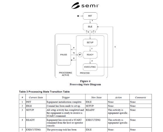
Identifying Custom Test Cases for the SEMI E30 GEM Standard: Part 1

How To Navigate the Settings Pages on the Brother™ Entrepreneur® Pro PR1000e
Solved If certain techniques are employed, an error of
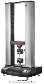
Mark-10 ES30 Manual Force Test Stand