The complete guide to PCB pad :types, size, spacing, repair and

Soldering is one of the most important processes in PCBA processing. On printed circuit boards, electrical connections to all components are made via PCB pads. The PCB pads are a very critical part of the PCB that determines where components are soldered on the PCB.The size, shape, and position of pads in a PCB directly depend on the manufacturing quality of the board. Today we will take a look at the PCB pad in SMT soldering.
Soldering is one of the most important processes in PCBA processing. On printed circuit boards, electrical connections to all components are made via PCB pad.

PCB Pad-to-Pad Spacing and Its Impact on DFM - VSE
DFA Rules Sierra Circuits

Getting to know PCB terminal blocks : function, material and sizes - IBE Electronics

LG Innotek launched the world's thinnest semiconductor package substrate - IBE Electronics

How to Calculate PCB Minimum Pad to Pad Spacing?

How to solve the solder scooped on welding? - IBE Electronics

What's the type of PCB surface treatment? - IBE Electronics

How To Repair Damaged /Missing PCB Pads INVISIBLE Fix, 45% OFF
What is Pad to Pad (PP) in PCB ?. Pad to Pad or PP is an important design…, by RayMingPCB
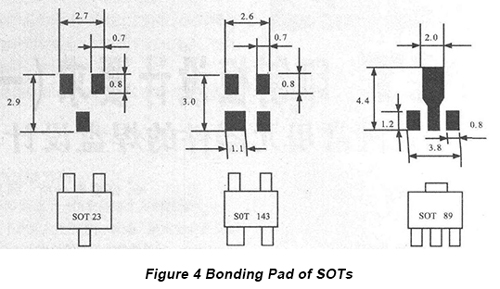
Design Requirement of SMT PCBs Part One: Bonding Pad Design of Some Ordinary Components

How To Repair Damaged /Missing PCB Pads INVISIBLE Fix, 45% OFF

PCB connector : definition, types, and how to choose and identify - IBE Electronics

PCB Pad-to-Pad Spacing and Its Impact on DFM - VSE

Energy storage PCB market embraces a broad development space under soaring new energy trends - IBE Electronics

PCB Pad Size Guidelines: Finding the Proper Pad Sizes for Your Circuit Design