Details of test chip designs: pad pitch, layout, materials, and opening.

Understanding the Importance of Prerequisites in the VLSI Physical Design Stage

Design and characterization of a copper-pillar flip chip test vehicle for small form-factor packages using 28nm ELK die and bump-on-trace (BOT)

PCB pad design principles
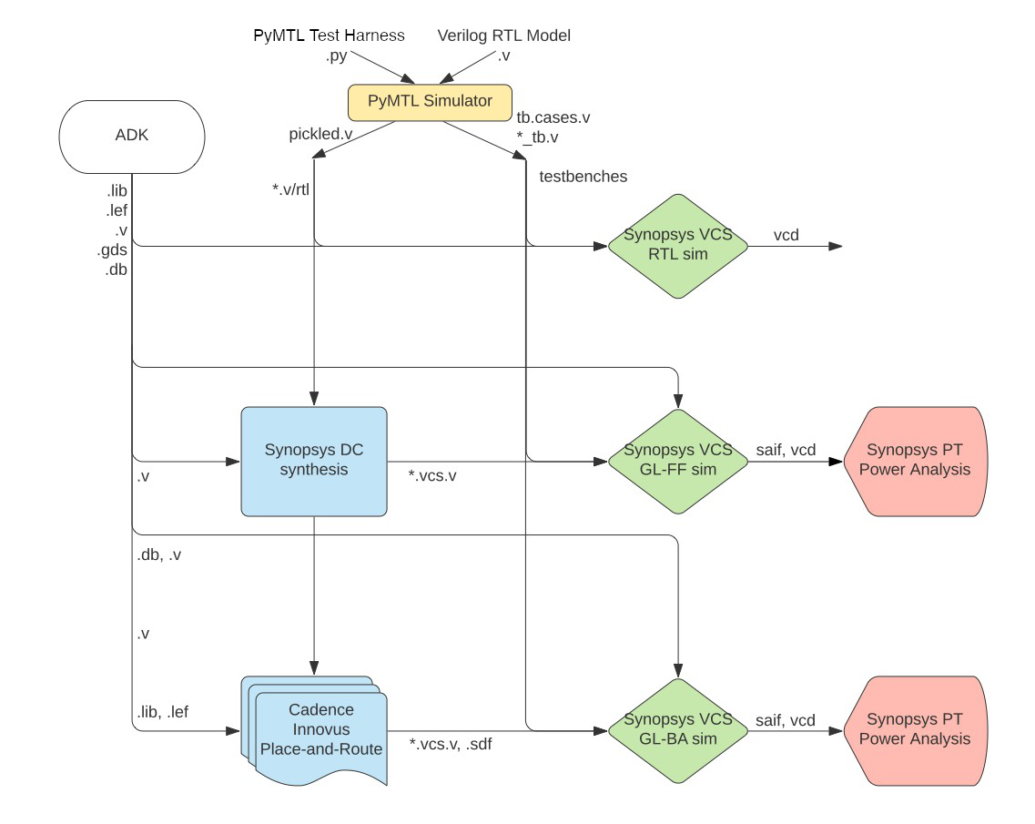
ECE 5745 Tutorial 4: Synopsys/Cadence ASIC Tools
Challenges Grow For Creating Smaller Bumps For Flip Chips
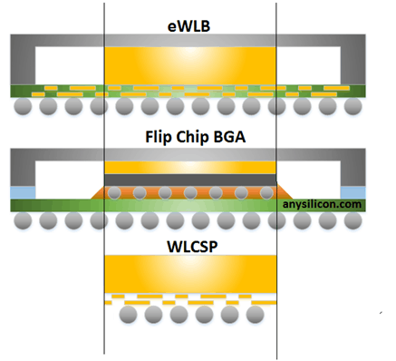
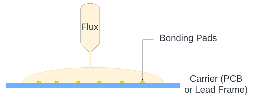
Understanding Wafer Bumping Packaging Technology - AnySilicon
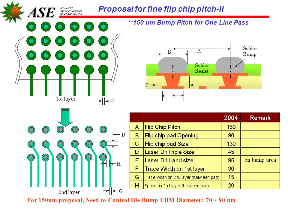
ASE Flip-Chip Build-up Substrate Design Rules - ppt video online download

Details of test chip designs: pad pitch, layout, materials, and opening.

How To Design A BGA, PDF, Printed Circuit Board

Shifting Left for Earlier Testing in 2.5D and 3D IC Design

Taking on the 0.3 mm ultra-fine pitch device challenge in PCB design
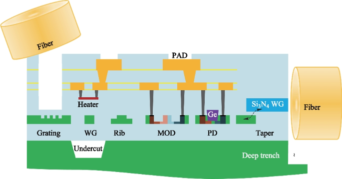
Co-packaged optics (CPO): status, challenges, and solutions
Flip Chip: The Ultimate Guide - AnySilicon