The bond pad redistribution layer (polyimide 1) and the under bump


Wafer level packaging having bump-on-polymer structure - ScienceDirect

Warren FLACK, Vice President, PhD

Figure 1 from Integrated 122-GHz Antenna on a Flexible Polyimide
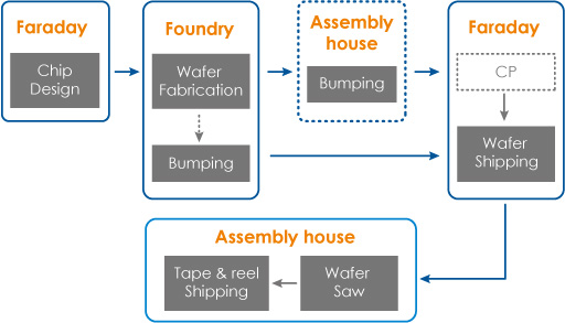
Faraday Technology Corporation-WLCSP Testing & Bumping Process

Comparison of conventional polyimide process and positive acting

Warren FLACK, Vice President, PhD

Chip Scale Packaging Helps Portable Medical Devices Save Size and
Polymers, Free Full-Text
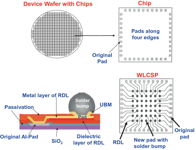
Fan-In Wafer/Panel-Level Chip-Scale Packages
PDF) Redistribution layers (RDLs) for 2.5D/3D IC integration

China HongRuiXing (Hubei) Electronics Co.,Ltd. latest

A review on numerical approach of reflow soldering process for

Bonding process of the ACF flip chip package; (a) before bonding

PDF) Characterization study of an aqueous developable