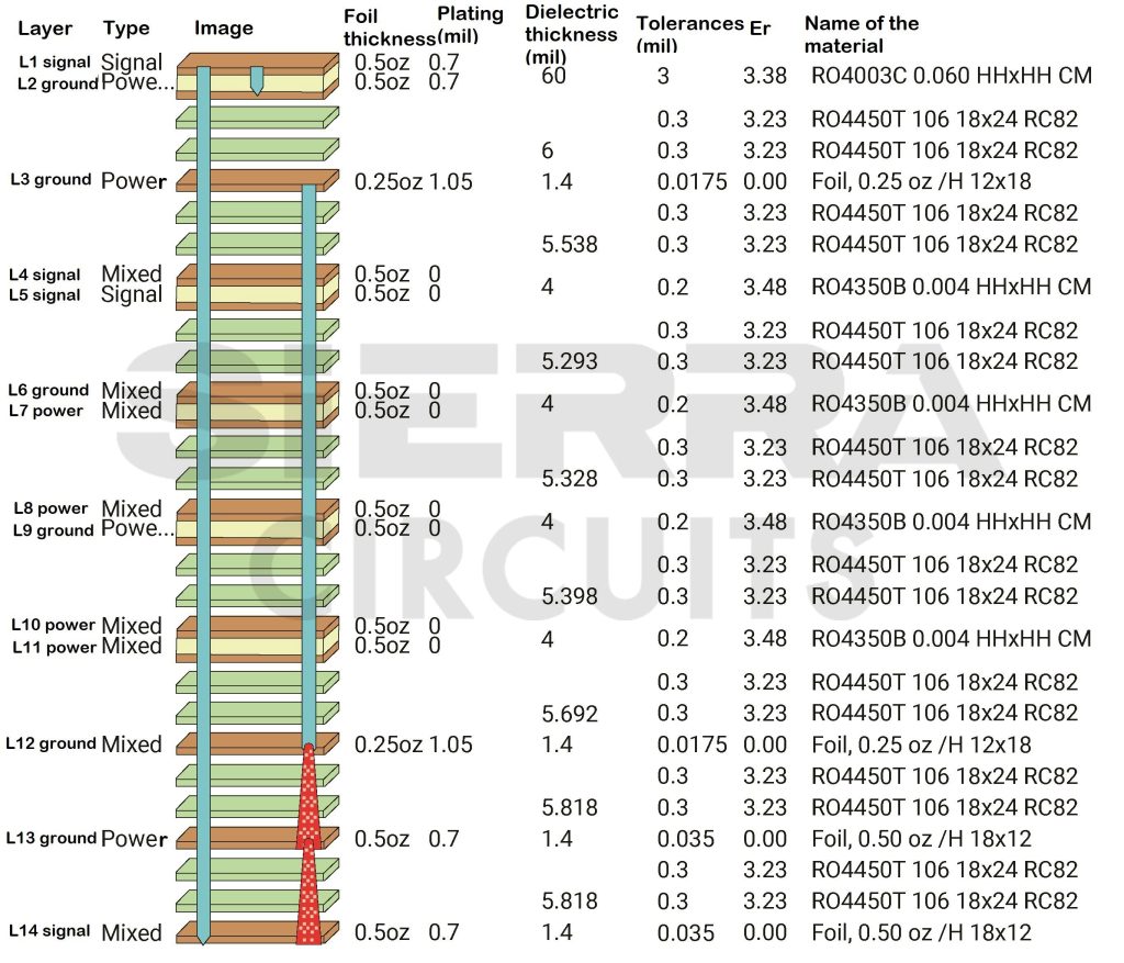
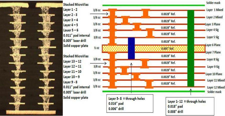
Case study: 8 and 14-layer HDI with Stacked Vias

This case study focuses on the challenges and solutions that we implemented to design complex HDI boards with stacked vias.
Case study: 8 and 14-layer HDI with Stacked Vias

How to Plan Multilayer PCB Stackup - RAYPCB
Designing HDI PCBs: The Requirements, Advantages and Complexities
Designing HDI PCBs: The Requirements, Advantages and Complexities

HDI PCB Stackup - Venture Elctronics

HDI PCB Stackup - Venture Elctronics

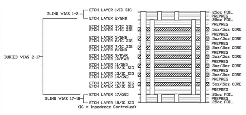
Explain Like I'm a Designer: ELIC PCB and HDI Routing, HDI Design

HDI PCB Stackup - Venture Elctronics

Understanding Proper PCB Design (Part 2) - Circuit Cellar

How to Design Your HDI PCB Stackup
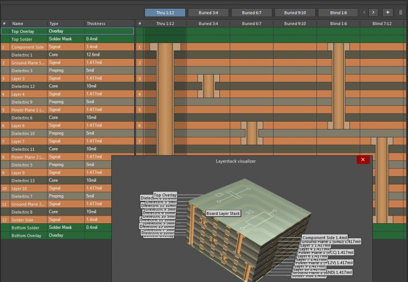
Advanced High Density PCB Design in Altium Designer

Understanding Proper PCB Design (Part 2) - Circuit Cellar
Microvia HDI PCB : All The Guidance You Need To Make The Right Choice