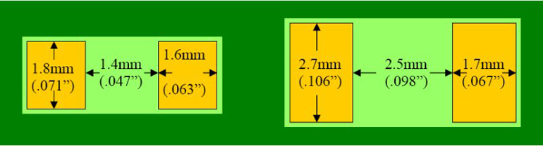
Details of test chip designs: pad pitch, layout, materials, and

Ball Grid Array Technology Overview
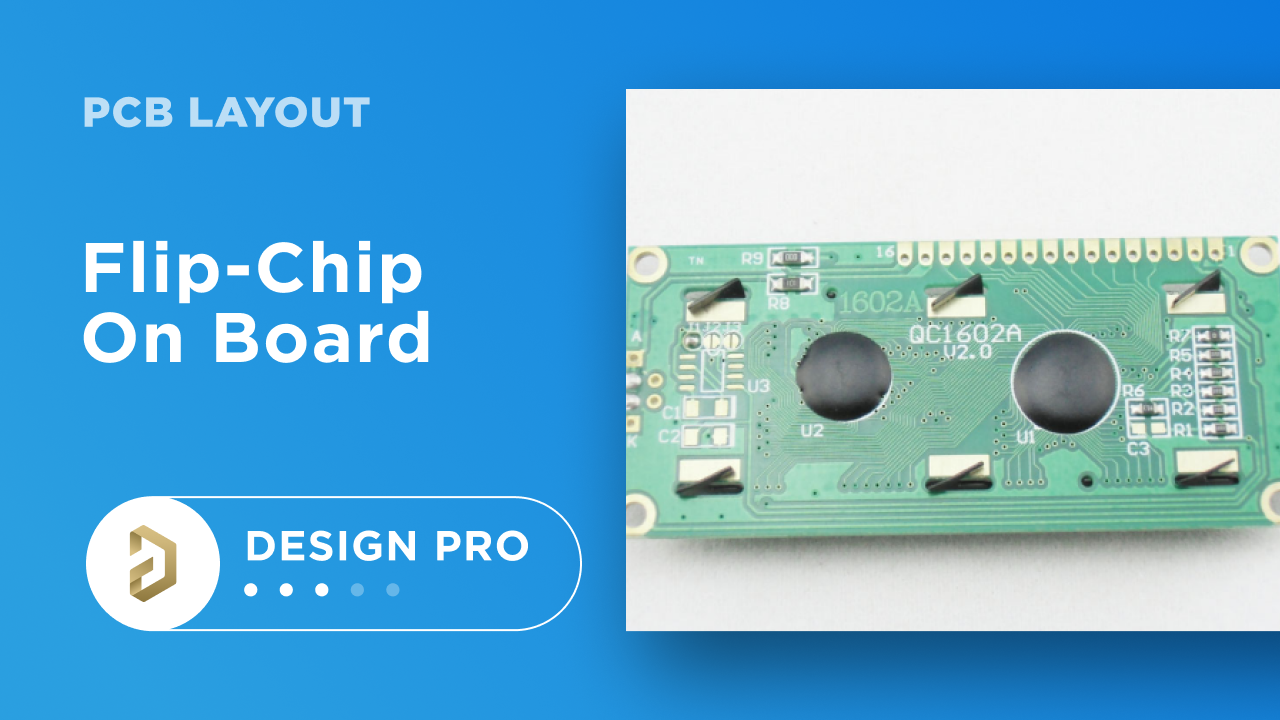
PCB Design Rules for Chip-on-Board Layout

FET Test Chips, Optimized for 2D Materials, Platinum
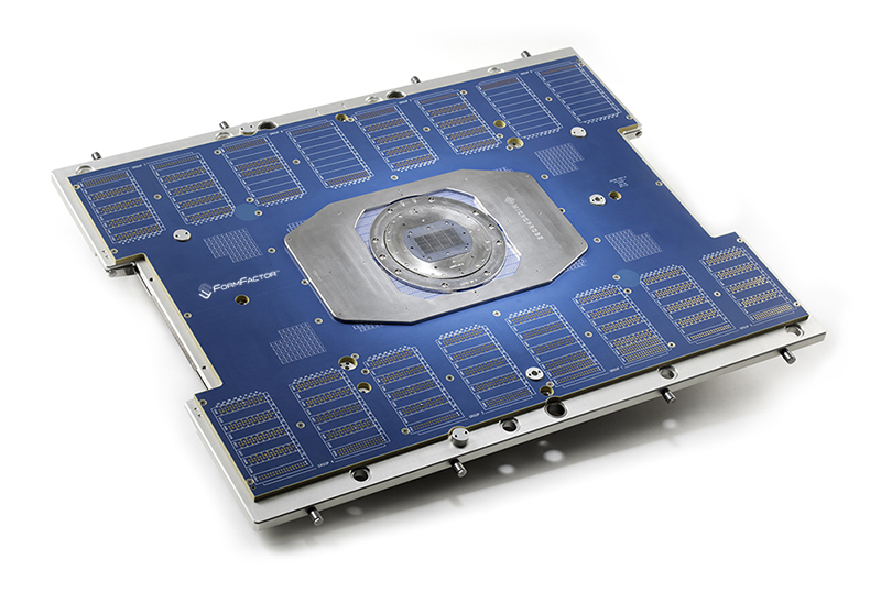
Apollo Vertical Probe Cards for Cu Pillar Test

Introduction of Plastic Ball Grid Array (PBGA) - FS PCBA

How to Design a BGA? - RAYPCB

Details of test chip designs: pad pitch, layout, materials, and opening.

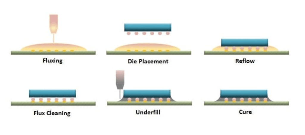
Squeegees in action to roll the paste and fill the stencil

AN-772: A Design and Manufacturing Guide for the Lead Frame Chip Scale Package (LFCSP)

Electronics, Free Full-Text
Advanced Packaging Part 2 - Review Of Options/Use From Intel, TSMC, Samsung, AMD, ASE, Sony, Micron, SKHynix, YMTC, Tesla, and Nvidia

What is a Pad in PCB Design and Development
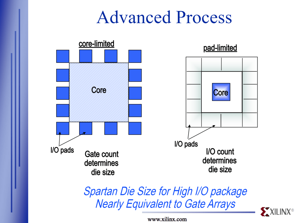
Advanced Packaging Part 1 – Pad Limited Designs, Breakdown Of Economic Semiconductor Scaling, Heterogeneous Compute, and Chiplets
Impact of Pad Design and Spacing on AC Breakdown Performance - Johanson Dielectrics
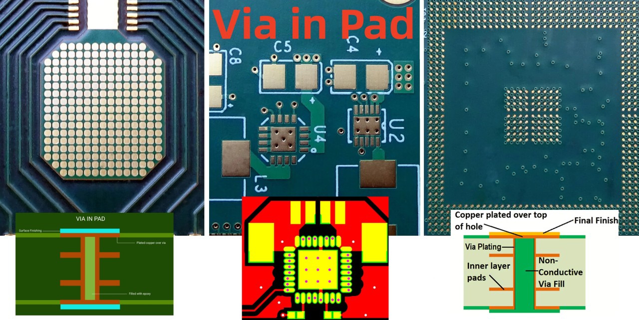
Via in Pad PCB Design